 Bars
Bars
 Beads & Spheres
 Bolts & Nuts
 Crucibles
 Discs
Discs
 Fibers & Fabrics
 Films
Films
 Flake
Flake
 Foams
Foams
 Foil
Foil
 Granules
 Honeycombs
 Ink
Ink
 Laminate
 Lumps
Lumps
 Meshes
 Metallised Film
 Plate
Plate
 Powders
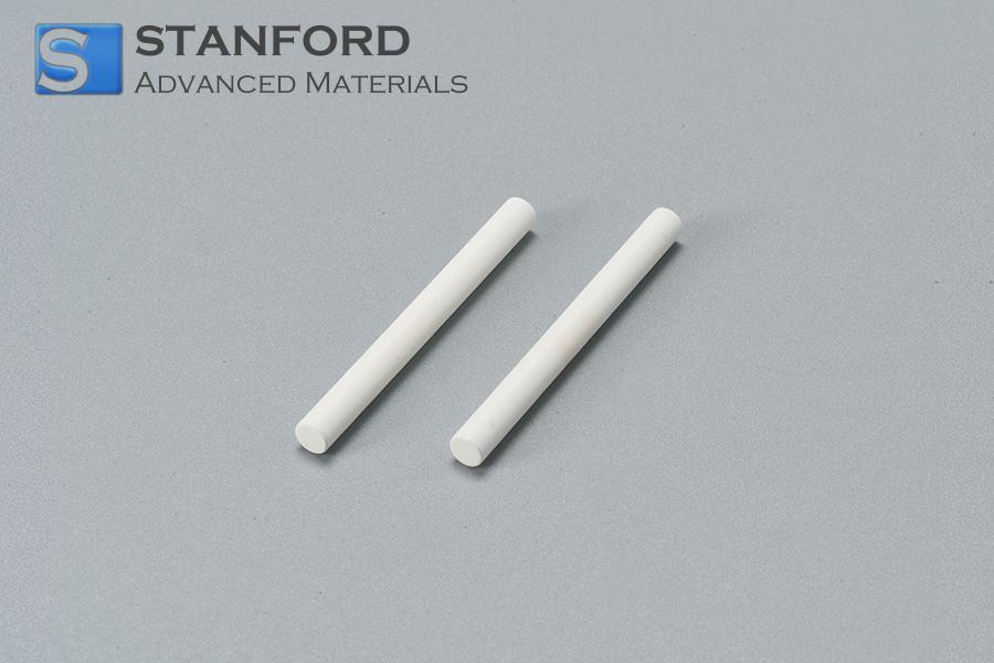
 Rod
Rod
 Sheets
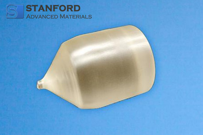
 Single Crystals
 Sputtering Target
 Tubes
Tubes
 Washer
 Wires
Wires
 Converters & Calculators
 Write for Us
Exploring The Properties, Manufacturing, And Applications Of Gadolinium Gallium Garnet
Introduction
Garnets belong to the mineral group A3B2(SiO4)3. They exhibit uniform physical properties and crystal structures. They are employed as gemstones, substrates and abrasives. However, garnets differ in chemical composition. This article addresses the garnet family with a focus on Gadolinium-Gallium Garnet (GGG) and reviews its properties, production method and applications. The text provides a basic understanding of this versatile material.
Definition of Gadolinium-Gallium Garnet
Gadolinium-gallium garnet (Gd3Ga5O12) is a synthetic garnet with well-defined thermal, mechanical and optical properties.
- Gadolinium-gallium garnet (GGG) has a thermal conductivity of 7,4 W m⁻¹K⁻¹ and a melting point of approximately 1 730℃.
- The material has a Mohs hardness ranging from 6,5 to 7,5.
- GGG exhibits an optical loss of less than 0,1 %/cm. It is transparent for optical components between 0,36 and 6,0 μm, and its refractive index ranges from 2,0 in the ultraviolet region to 1,8 in the infrared region.
Production of Gadolinium-Gallium Garnet
The Czochralski method is a well-established technique for growing single crystals, including Gadolinium-Gallium Garnet (GGG). Jan Czochralski, a Polish scientist, discovered this method when a seed was inadvertently immersed in molten tin. This observation led to its adoption for single crystal production.
Figure 1 presents a schematic diagram of the Czochralski process as applied to silicon crystal production.
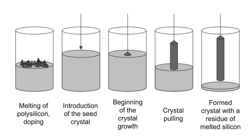
The process comprises the following steps:
-
The starting material is heated in a round crucible until it is completely molten.
-
A seed crystal is carefully introduced into the melt while being rotated slowly, thereby initiating crystal formation.
-
The seed crystal is slowly withdrawn from the melt, and a single crystal develops at the interface.
The Czochralski method requires precise control over process parameters. Temperature, rotation speed and withdrawal speed are monitored to ensure the desired crystal quality and shape. An inert atmosphere is maintained to prevent contamination and oxidation.
Dopants may be added to adjust colour or other specific properties. The method is also used for the production of semiconducting materials such as silicon and gallium arsenide.
Applications of Gadolinium-Gallium Garnet
Gadolinium-gallium garnet is employed in various sectors due to its precisely determined properties. It is used as a substrate material for magneto-optical layers. Depositing a Yttrium-Iron Garnet film on a GGG substrate facilitates the production of optical infrared isolators.
GGG is used as a carrier for magnetic bubble memory, given that its lattice parameter closely matches that of the storage material. GGG crystals are also employed as substrates for microwave isolators.
During the 1970s, GGG was used as a diamond simulant owing to its optical resemblance to natural diamonds. It was subsequently replaced by Yttrium-Aluminium Garnet (YAG) because YAG exhibits a higher hardness. GGG continues to be selected when a diamond-like appearance is required.
Other Garnet Materials
Our website provides several options for synthetic garnets. One option is Cerium-doped Gadolinium-Aluminium-Gallium Garnet (Ce:GAGG). It displays a high light yield, a rapid scintillation response, chemical stability and high energy resolution. Ce:GAGG is suitable for X‑ray imaging, computerised tomography (CT) and other medical imaging techniques.
Another option is Neodymium-doped Yttrium-Aluminium Garnet (Nd:YAG), which demonstrates high optical absorption and energy conversion efficiency. Nd:YAG is used in laser marking devices, cosmetic instruments and cutting machines.

Please visit our homepage for further information.
Further details: An Introduction to 7 Types of Synthetic Garnet Materials
Conclusion
Gadolinium-Gallium Garnet (GGG) is a material with defined properties, including a high melting point, thermal conductivity, hardness and measured optical characteristics. At Stanford Advanced Materials (SAM) we offer high-purity garnets in various diameters to meet specific requirements. If you are interested, please send us an enquiry and we will provide further assistance.

 Chin Trento


